

Using specially-engineered metamaterials, researchers at the University of California San Diego (UC San Diego) have created the world's first microelectronic device that does not use semiconductors, but instead employs low-power laser optical control to increase its conductivity by more than 1,000 percent.
According to the UC San Diego team, transistors and other common semiconductor devices have an upper limit to their conductivity properties due to the restrictions inherent in the materials from which they are made. This is because a semiconductor's band gap (the set amount of energy needed for an electron to break free from the material and flow along a conduction path) means that extra energy is needed to allow electron flow. In addition, the velocity of electrons is limited in semiconductors as they collide with atoms while they move through the materials.
These limitations to conductivity are what the researchers at UC San Diego looked to eliminate by exchanging semiconductors with a metamaterial that allowed electrons to flow freely through open space.

Ordinarily, moving electrons from materials and into free space isn't all that easy and needs the application of at least 100 volts, excitation with high-power lasers, or heating to temperatures in excess of 1,000° F (538° C), all of which are fairly impractical in miniature electronic devices.
To overcome such extreme requirements, the team used specialized surfaces, known as metasurfaces, to engineer a microscale device that can release electrons via localized surface plasmon resonances (essentially the generation of electric fields near the surface of the material's particles that provide low-loss conduction paths).
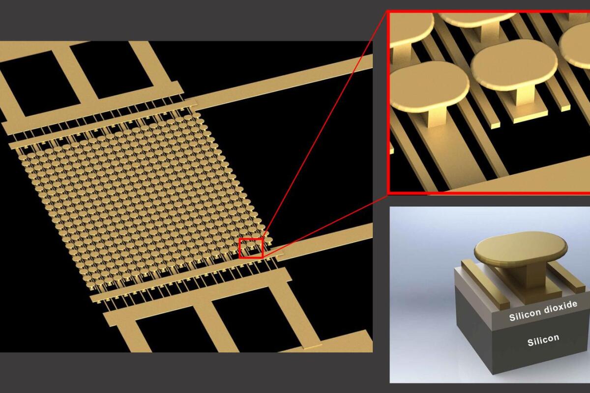
Created from an array of gold mushroom-shaped nanostructures mounted on a matrix of gold strips and built on top of a silicon wafer with a layer of silicon dioxide separating the two levels, the metasurface generates "hot spots" of high intensity electric fields when a low DC voltage (under 10 volts) and a low power infrared laser are simultaneously applied.
This voltage and laser excitation in turn produces enough energy to free electrons from the metamaterial, which can then flow freely through space. So much so, tests showed that a greater than 1,000 percent change in conductivity occurred.
"That means more available electrons for manipulation," said Ebrahim Forati, a former postdoctoral researcher on the project at UC San Diego.
Metasurfaces are being seen in many more miniature prototype devices, such as in ultrathin lenses that manipulate light in ways that conventional optics can't or passive acoustic sound absorbers that are able to redirect sound energy unlike any other acoustic appliance, because they are able to mechanically influence the wavelengths of phenomena without having to resort to the addition of high-powered electronic components.
"This certainly won't replace all semiconductor devices, but it may be the best approach for certain specialty applications, such as very high frequencies or high power devices," said Professor Dan Sievenpiper, head of the research team at the Applied Electromagnetics Group of UC San Diego.
This specific metasurface was created as a proof-of-concept, and not a generic component, so the team believes that different metasurfaces will have to be tailored for other devices and possible uses in such fields as photochemistry and photocatalysis, as well as enabling new types of photovoltaic devices.
"Next we need to understand how far these devices can be scaled and the limits of their performance," said Sievenpiper .
The results of this research were recently published in the journal Nature Communications.
The short video below was produced by UC San Diego to further explain the research.
Source: UC San Diego