
Researchers from the University of Minnesota and Seoul National University have developed a new lithographic method with the help of a very low-tech tool: Scotch Magic tape. This new method, which promises to enhance our ability to fabricate nanostructures, has been used to build highly nonlinear optical materials consisting of sheets of 25 micron (0.001 in) metal blocks separated by nanometer-wide insulating channels. As light squeezes through these channels, incompletely understood plasmonic effects enable novel optical behavior.
Richard Feynman popularized the idea that the future of technology lay in the assembly of individual atoms into novel constructs in his 1959 essay There's Plenty of Room at the Bottom. However, more than a half-century later, the ability of nanofabrication to provide engineers with new materials having novel structures and properties is still seriously limited compared to the dream of molecular nanoassemblers that could make, literally, anything physically possible from raw material and energy. Accordingly, any substantial increase in our ability to fabricate nanostructures is, if not an earth-shaking breakthrough, a very welcome state of affairs indeed.
Surprisingly, the use of Scotch tape in the production of advanced materials has a long history, ranging from its use in production of lift-off semiconductor structures in the 1980s through the 2004 Nobel-Prize winning discovery in which graphene layers were isolated by peeling them from graphite using Scotch tape.
The new method allows construction of precise metal layers having a bespoke substructure of nanometer insulating layers. Such nanostructured materials possess highly unusual optical properties, but just how are such materials fabricated?
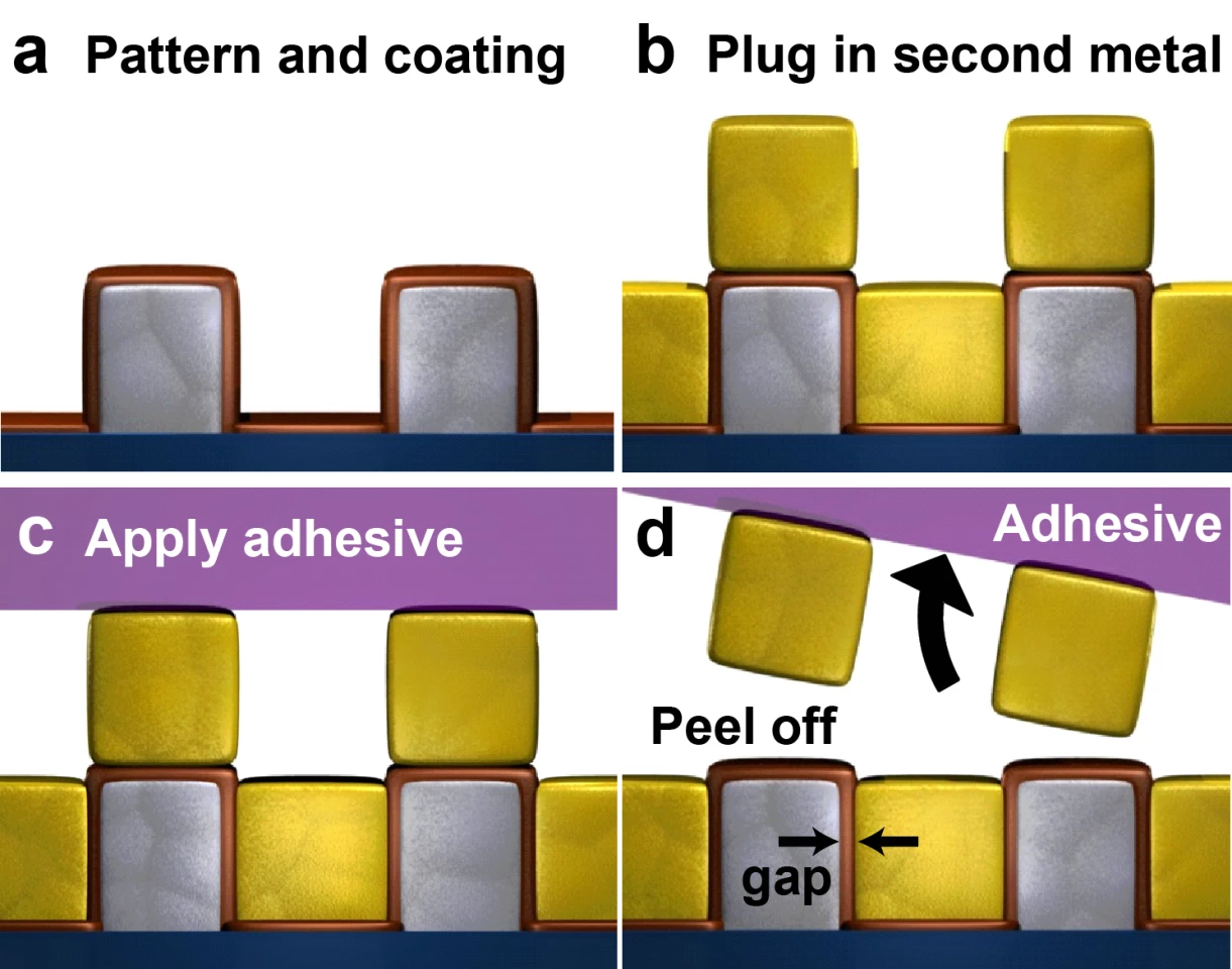
A metal layer (gray) is grown on a silicon substrate, and then is structured into a matrix of 25 micron (0.001 in) metal squares located on 50 micron (0.002 in) centers using standard lithographic methods. A layer of alumina only a few atomic layers in thickness (red) is then deposited on the metal islands using atomic layer deposition (ALD). ALD grows a material (in this case alumina) one atomic layer at a time, leading to defect-free nanometer thick layers of essentially constant thickness ALD. The result is a conformal coating, meaning that all exposed surfaces receive the same thickness and quality of coating. The result is shown as structure a above.
Now a thick layer of a second metal (yellow) is grown on top of structure a. The two metal layers can be made of the same or differing materials, as desired for the effects being studied. The top layer is deposited by sputtering or vacuum deposition, so that the new metal layer is not conformal, but rather grows strictly atop the existing structure. The result is structure b, which is essentially a single nanostructured layer of metal islands separated from a surrounding sea of metal by nanometer thick layers of alumina. Atop this nanostructured layer is a pattern of isolated 25 micron (0.001 in) metal islands, whose anchorage is a nanometer-thick layer of alumina.
Now comes the tricky part. The top layer of metal islands are just in the way (at least for one class of interesting nanostructured materials), so must be removed without damaging any of the insulating nanogaps in the lower layer.
Easier said than done. You can try chemical, physical, and/or mechanical polishing and etching techniques, but a specific method to remove the excess metal while preserving the integrity of essentially all the horizontal nanoscale gaps had proven extremely elusive. The discovery that Scotch Magic tape was a nearly perfect tool for removing the excess metal islands was, perhaps, less surprising than that one of the researchers decided to attempt its use.
To remove the islands, the Scotch Magic tape is applied to the structured layers to produce structure c. The tape is too stiff to allow the adhesive to contact the bottom, fully nanostructured layer, so only adheres to the tops of the excess metal islands on the top of the structure. Finally, as shown in d, when the tape is removed from the substrate, it takes with it the top layer of metal islands without damaging the bottom layer.
But why do the metal islands detach cleanly and thoroughly without damaging the underlying nanostructured layer? The interface between the first metal islands and the alumina nanolayer is nearly perfect, and hence quite strong, owing to having been grown via ALD. On the other hand, the interface between the top of the alumina layer and the excess metal islands is not nearly as strong. When torque is applied to the islands by peeling of the tape, the faulty interface simply breaks, and the excess islands are cleanly removed.
The research team tested the integrity of the insulated nanochannels using a tunneling method. If you look at structure d in the figure, the gray metal islands are in contact with the substrate, which is a conductive silicon wafer. While contact can be made with the yellow metal layer from above, in a perfect structure there is no direct electrical path between the two sides of the structure.
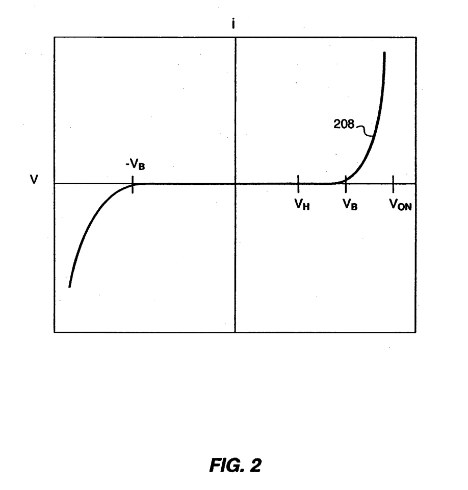
This can be tested by connecting a voltage across the wafer and the yellow metal layer, and measuring the electric current. If the insulating nanogaps are broken, the amount of current will be proportional to the voltage in accord with Ohm's law. If the nanogaps areas intact, there will be virtually no current seen until the voltage reaches a level at which tunneling currents are stimulated, as shown in the image above. Nearly perfect tunneling behavior was found, demonstrating the extremely high quality of the new nanostructures.
Perhaps the most striking of the unusual optical properties of such nanogapped materials is their transparency. In classical optics, thick metal layers are fully opaque. Further, light cannot easily be squeezed into regions much smaller than a wavelength in either classical or quantum optics. Those two observations put together suggest that a nanogapped metal layer should be completely non-transparent.
However, this turns out not to be the case – light passes easily through the nanogapped layer, which is about as thick as aluminum foil. So which of the two ideas above was the misleading one?
Actually, they are both true, but so is a third concept. When a photon travels close to a metal surface, the electrons near the metal surface begin to move back and forth in response to its oscillating electromagnetic field. Producing this interaction actually requires that the photon be repeatedly absorbed and re-emitted, which greatly slows the apparent speed of the photon. In essence, the photon merges with the mechanical vibrations of the metal's electrons to form a quasiparticle called a surface plasmon polariton (SPP). The field of engineering that describes properties and application of such excitations is called plasmonics.
Plasmonics produces novel properties in materials because, while the frequency of the vibrations remains that of the original photon, the slower speed of the SPP means that the wavelength of the SPP (speed/frequency) is far smaller than that of the original photon. The reduction in wavelength is roughly a few thousandfold, from microns to nanometers. These far smaller SPPs can pass right through the nanogaps in the metal layers.
The small dimensions of the SPPs also lead to extremely large electric and magnetic fields within and near the nanogaps. This leads to insanely large refractive indices, as well as left-handed (negative) refraction, and a range of novel methods for active and passive control of optical flow through plasmonic devices analogous to the semiconductor devices used in electronics.
The research was detailed earlier this year in Nature Communications.