Despite their ability to generate clean, green electricity, solar panels aren't as commonplace as the could be. The main sticking point, of course, is price. Due to their need for relatively expensive semiconductor materials, conventional solar cells don't yet have a price-efficiency combination that can compete with other sources of electricity. Now Profs. Alex Zettl and Feng Wang of Lawrence Berkeley National Laboratory and the University of California at Berkeley have developed seriously unconventional solar cell technology that allows virtually any semiconductor material to be used to create photovoltaic cells.
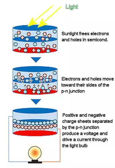
A solar cell works according to these steps. First, sunlight hits the solar cell and is absorbed by the semiconductor of which the solar cell is made. In the absorption process, electrons are freed from their atoms, allowing them to flow through the semiconductor. The presence of a p-n junction acts as a diode, only allowing the electrons to move in a single direction. (Electrons and holes move in opposite directions, but the electrical current only moves in one.) Metal electrodes then transfer the light-generated electron flow into an electric circuit for use. A p-n junction is the interface between a region of the semiconductor where the dominant charge carriers are holes and a region where the carriers are electrons.

A conventional solar cell is made of a thin wafer of a semiconductor with a metallic electrode deposited on its rear side. The side facing the light source is polished more finely than any optical lens, cleaned to the atomic level, and then dopant atoms are deposited onto the front side, whereupon the entire wafer is placed in a high-temperature diffusion furnace.
The purpose of a dopant is to change the dominant charge carrier in the semiconductor from hole-rich to electron-rich, or v.v. In this process the p-n junction that converts incident light into a flow of electrons is formed. Following diffusion, the wafer is again cleaned, and a metallic electrode is grown on the front surface, using arcane rituals to ensure an ohmic contact with the active semiconductor material. (An ohmic contact is an electrical contact that obeys Ohm's law, having no rectifying or diode-like properties.)
The efficiency of conventional solar cells is also limited by the semiconducting materials which are suitable for the manufacture of solar cells by some approximation of the above process. It must be possible for the dominant charge carrier of the semiconductor to be changed between p (hole) and n (electron)-dominated conduction by introduction of chemical dopants, so that a well-behaved p-n junction is formed. It must also be possible to make a satisfactory electrical contact between the electrodes and the semiconductor.
There are many semiconductor materials with optical properties and electronic band-gaps well suited to conversion of light to electricity for which one or another of the rather rigid criteria for manufacture of conventional solar cells fails. These include many metal oxides, sulfides and phosphides, which are plentiful and inexpensive, but have been considered unsuitable because it is so difficult to alter their electronic structure chemically (e.g., through doping). For example, zinc oxide is a semiconductor well suited for capturing violet and near ultraviolet light, which is wasted by most conventional solar cells.
We now have Zettl and Wang's unconventional solar cells. Broken down, the expensive parts of making regular solar cells are the semiconductor wafer, forming a high-quality p-n junction under the surface of the wafer, and making ohmic electrical contact with the front and back of the wafer. Aside from providing a semiconductor wafer (usually of a cheaper material), the new solar cells require none of this.
The new technology is called "screening-engineered field-effect photovoltaics" (SFPV). An electrode is deposited on the front of the semiconductor wafer, which partially screens the semiconductor from an electric field generated between the front and rear electrodes. Assume the semiconductor is naturally p-type, so that it has an excess of holes. The applied electric field then penetrates the semiconductor surface slightly, attracting electrons toward the surface and repelling holes. As a result, the semiconductor near the surface changes from p-type to n-type (electron-rich), and a buried p-n junction has been generated – not by chemistry, but by use of carefully tailored electric fields. An extra bonus is that the front electrode automatically forms an ohmic contact with the semiconductor wafer.
“Our technology requires only electrode and gate deposition, without the need for high-temperature chemical doping, ion implantation, or other expensive or damaging processes,” said lead author of a paper describing the new technology, William Regan. “The key to our success is the minimal screening of the gate field which is achieved through geometric structuring of the top electrode. This makes it possible for electrical contact to and carrier modulation of the semiconductor to be performed simultaneously.”

Two electrode configurations that exhibit the SFPV concept have been developed. In one, the electrode in contact with the semiconductor wafer is formed of a row of narrow fingers, while in the other the partial screening is accomplished by placing a layer of graphene atop the semiconductor wafer. In both cases, high-quality p-n junctions are formed in semiconductors for which this structure was previously impossible.
Low cost, high efficiency solar cells? Sounds like a winner here – let's see when and if it hits the market.
The team's research is published in the journal Nano Letters.


