Researchers at MIT have unexpectedly stumbled upon a way to 3D print active electronics – meaning transistors and components for controlling electrical signals – without the use of semiconductors or even special fabrication technology.
That goes far beyond what we can currently do with 3D printers. And if perfected, this method could eventually spell the beginning of a new wave in prototyping, experimentation, and even DIY projects for tinkerers at home.
With 3D printing, any of a range of materials including thermoplastic filaments, resin, ceramic, and metal, are laid down in successive thin layers to form a three-dimensional object. That means you can print all kinds of things, from action figures to jewelry to furniture to buildings.
So why don't we 3D print working electronics? The major challenge is that semiconductors, which are traditionally made of pure silicon and cut into thin wafers to be made into chips for gadgets, are extremely fragile. Their functionality can be affected by dust, airborne particles and microbes, and even temperature and humidity. As such, they're handled carefully in cleanrooms, where air quality and other factors are strictly controlled to ensure the chips fabricated inside work precisely.
Plus, modern chip design is extremely complex, with millions or billions of transistors crammed onto tiny processors using nanometer-scale processing technologies. That's far more precise than what we can currently achieve with standard 3D printers.
For reference, IBM's Gekko chip that powered the Nintendo GameCube in 2001 had 21 million transistors. The Apple A12 Bionic chip in the 2018 iPhone XS had 6.9 billion transistors, and was manufactured using a 7-nanometer process technology.
To be clear, 3D printing modern gadgets is not at all what the MIT researchers were going for. In fact, they didn't even have semiconductors on their minds when they figured this out.
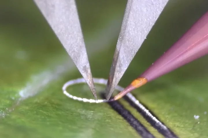
The researchers were fabricating magnetic coils using a process called extrusion printing for another project. It was then that they observed that the material they were using – a polymer filament doped with copper nanoparticles – would exhibit a large spike in resistance when they passed electric current through it. And as soon as they turned off the current, the material's resistance dropped back to normal.
That's essentially the property we see in semiconductors like silicon. It's why we use them to make transistors that switch on and off to form logic gates in processors.
“We saw that this was something that could help take 3D printing hardware to the next level,” said Luis Fernando Velásquez-García, principal research scientist at MIT’s Microsystems Technology Laboratories. "It offers a clear way to provide some degree of ‘smart’ to an electronic device."

The team demonstrated fully 3D-printed resettable fuses and transistors using this inexpensive material. These are simple, albeit essential components in electronic devices that typically use hard-to-handle semiconductors.
At a few hundred microns in size, these transistors are not nearly as small or performant as the ones you'd find on an iPhone processor. However, they are durable, and can be used for a range of simple applications. That includes something as straightforward as a switch to operate a motor, and to turn into parts for integrated circuits.
“The reality is that there are many engineering situations that don’t require the best chips," said Fernando Velásquez-García. "At the end of the day, all you care about is whether your device can do the task. This technology is able to satisfy a constraint like that.”
With a biodegradable material and no need for cleanrooms, this method for making simple electronics could find use in places where high-end fabrication is difficult – like remote research labs and "on board spacecraft."
Now that's what I call a happy accident. A paper on the research has been published in the journal Virtual and Physical Prototyping.
Source: MIT News