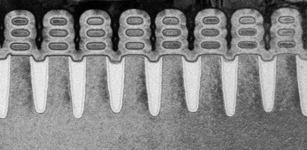
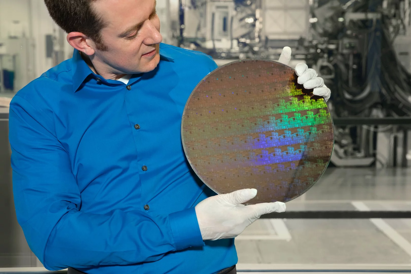
The smallest and most advanced chips currently commercially available are made up of transistors with gates about 10 nm long, but IBM has now unveiled plans to cut them in half. To create 5 nm chips, the company is ditching the standard FinFET architecture in favor of a new structure built with a stack of four nanosheets, allowing some 30 billion transistors to be packed onto a chip the size of a fingernail and promising significant gains in power and efficiency.
First coined in the 1970s, Moore's Law was the observation that the number of transistors on a single chip would double every two years. The trend has held up pretty well ever since, but the time frame of the doubling has slowed down a little in recent years. In consumer electronics, 14 nm chips are still stock-standard, but advances from the likes of Intel and Samsung mean that 10 nm versions have started hitting the high-end market.
But the march of technology never stops, and in 2015 IBM unveiled a 7 nm test chip, developed in conjunction with GlobalFoundries and Samsung. This prototype crammed some 20 billion transistors onto a fingernail-sized chip, thanks to some new manufacturing tricks and materials, and they're expected to be rolled out on a commercial scale in about 2019.
Now, the same group of companies has unveiled the next step beyond that. With individual switches just 5 nm in diameter, an extra 10 billion of them can be squeezed onto a chip the same size. While current manufacturing techniques could potentially shrink down to the 5 nm scale, the team instead developed a brand new architecture.
Semiconductors have been made using the FinFET architecture since about 2011. As its name suggests, these transistors are fin-shaped, with three current-carrying channels surrounded by an insulating layer. But, as often happens with technology, this structure is starting to bump up against the limits of how small it can be scaled, and the IBM team says shrinking the fins any further won't do much to improve their performance.

Instead, the 5 nm chips are made using stacked silicon nanosheets, which can send signals through four gates at once, instead of FinFET's three. They're created using Extreme Ultraviolet (EUV) lithography, a process that writes patterns on a silicon wafer using a much higher energy wavelength of light than the current technique. That means finer details can be created on the chip, and unlike existing lithography processes, the chips' power and performance can be adjusted continuously during manufacturing.
Compared to the current 10 nm chips, the 5 nm prototypes are capable of improving performance by 40 percent at fixed power, or provide a power saving of 75 percent at matched performance. The development could lead to smaller, more powerful and more efficient devices – but with 10 nm chips only just hitting the market, and 7 nm due for commercial release in 2019, these 5 nm chips are probably still about four years away.
Source: IBM


