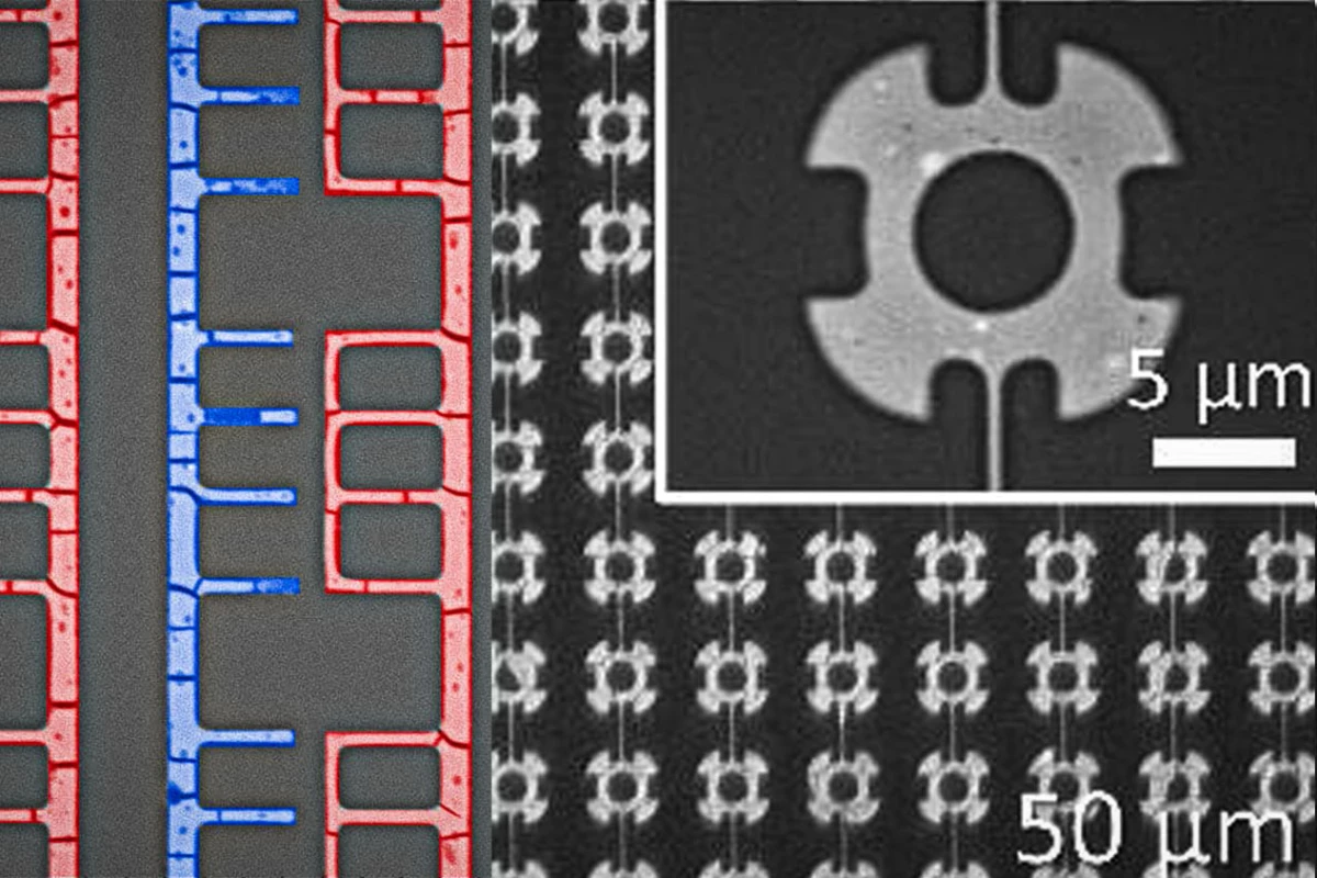
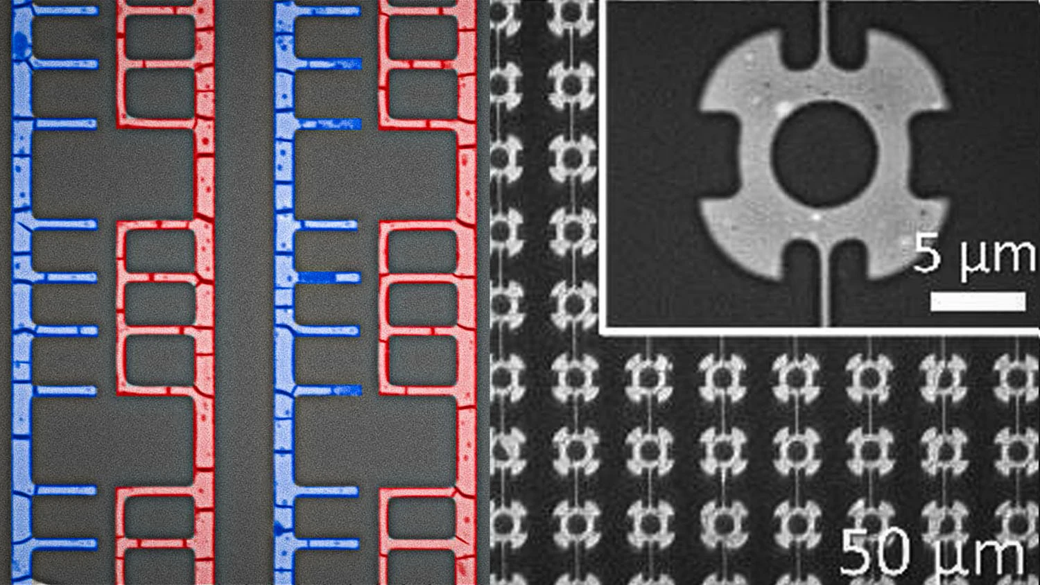
A remarkable proof-of-concept project has successfully manufactured nanoscale diodes and transistors using a fast, cheap new production technique in which liquid metal is directed to self-assemble into precise 3D structures.
In a peer-reviewed study due to be released in the journal Materials Horizons, a North Carolina State University team outlined and demonstrated the new method using an alloy of indium, bismuth and tin, known as Field's metal.
The liquid metal was placed beside a mold, which the researchers say can be made in any size or shape. As it's exposed to oxygen, a thin oxide layer forms on the surface of the metal. Then, a liquid is poured onto it, containing negatively-charged ligand molecules designed to pull individual metal atoms off that oxide layer as positively-charged ions, and bind with them.
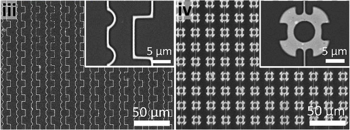
These metal ions held in the ligands become a little like magnetic building blocks, attracted to one another, and as the ligand solution begins to flow through channels in the mold, driven by capillary action, it pulls these building blocks through with it. The mold essentially gets the blocks to line up into orderly structures, like wires, and stick to each other in place.
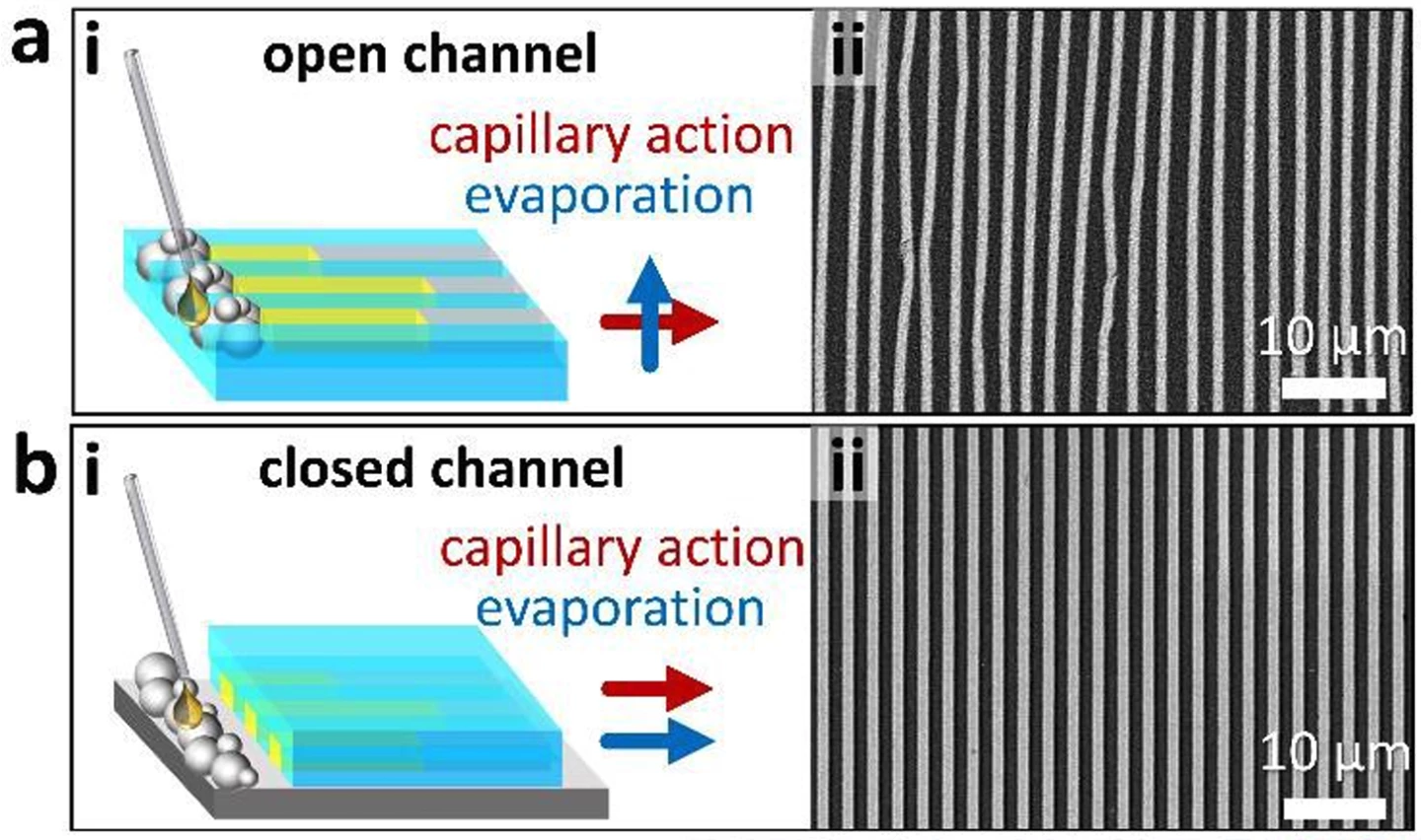
“Without the mold, these structures can form somewhat chaotic patterns,” says Martin Thuo, corresponding author and professor of materials science and engineering at North Carolina State University. “But because the solution is constrained by the mold, the structures form in predictable, symmetrical arrays.”
Once everything is in place, the liquid part of the ligand solution begins to evaporate, which has the effect of squeezing the ligands and metal ions even closer together in their channels. Then the mold is taken away, and the final shape is slowly heated to around 600 °C (1,112 °F) and kept there for an hour.
This heating process supplies enough energy to break the chemical bonds holding the ligand molecules together, so carbon and oxygen atoms are released.
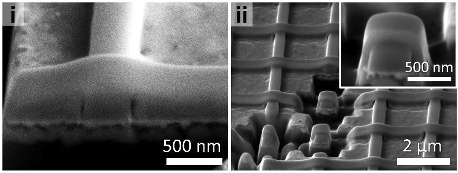
The oxygen immediately bonds to the metal ions, forming semiconductor metal oxides that fuse together with one another in a sintering process to form wires. The carbon atoms, meanwhile, organize themselves into graphene, which wraps neatly around the wires to improve their electrical conductivity, protecting them from moisture or further oxidation.

The researchers demonstrated they can also use these graphene layers to tweak the electrical and optoelectric properties of the resulting wires. “The graphene sheets can be used to tune the bandgap of the semiconductors, making the semiconductor more or less responsive, depending on the quality of the graphene,” says Julia Chang, first author of the paper and a postdoctoral researcher at NC State.
Even though the heating process causes "severe volume shrinkage," the resulting wires remain continuous and don't break.
“In short, we’ve shown that we can self-assemble highly structured, highly tunable electronic materials for use in functional electronic devices,” says Thuo. “This work demonstrated the creation of transistors and diodes. The next step is to use this technique to make more complex devices, such as three-dimensional chips.”
“The nature of the D-Met (directed metal ligand) technique," he continues, "means you can make these materials on a large scale – you’re only limited by the size of the mold you use."

The team says the technique offers a faster, cheaper, more reliable way of making computer chips. “Existing chip manufacturing techniques involve many steps and rely on extremely complex technologies, making the process costly and time consuming,” says Thuo. “Our self-assembling approach is significantly faster and less expensive. We’ve also demonstrated that we can use the process to tune the bandgap for semiconductor materials and to make the materials responsive to light – meaning this technique can be used to create optoelectronic devices.
“What’s more, current manufacturing techniques have low yield, meaning they produce a relatively large number of faulty chips that can’t be used. Our approach is high yield – meaning you get more consistent production of arrays and less waste.”
It's a pretty remarkable piece of work – but in the electronics game, size is key. Take a quick scan through the remarkable video below to get a sense for just how tiny the 'wires' in a modern CPU chip need to be.
The state-of-the-art production techniques used by manufacturers like Taiwan's TSMC can produce features with minimum dimensions as small as 3 nm – or about the width of 15 individual silicon atoms. It's absolutely staggering that this mass-manufacturing is happening so close to the individual-atom scale, but the smaller it gets, the faster and more efficient the resulting chip can become.
How does this 'self-assembling' technology stack up against that? Well, in the published study, the researchers managed to successfully fabricate wires from about 1,000 nm all the way down to 44 nm.

That's pretty incredible; this is a proper nanoscale-capable manufacturing technique that's faster, cheaper and more reliable than today's best methods, even if it can't yet compete on atomic-scale final resolution. It's unclear whether the D-Met technique can be adapted to work at even smaller scales – but the research team believes it's well and truly capable of scaling up in terms of mass production.
The paper is open access, post-peer review and pre-publication in the journal Materials Horizons.
Source: North Carolina State University

