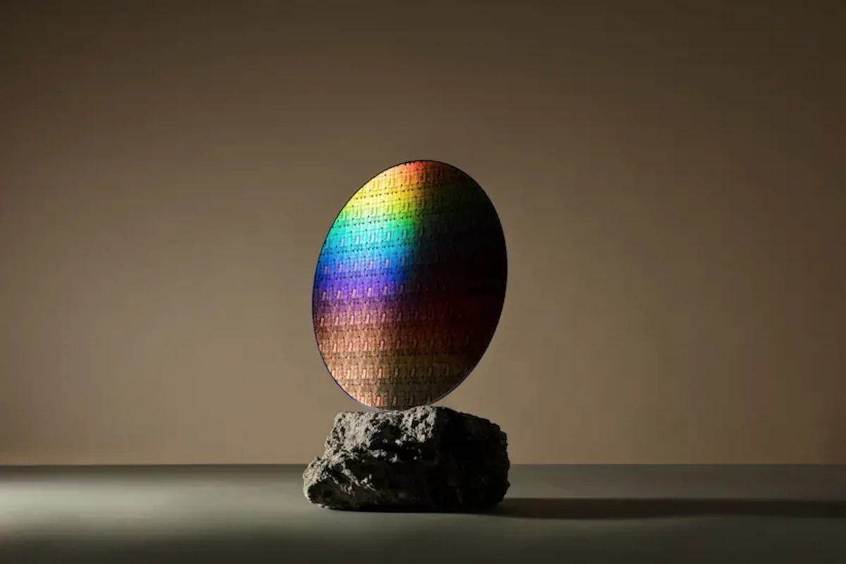
IBM and Samsung have unveiled a new semiconductor chip design they say can enable the continuation of Moore's Law. The breakthrough architecture sees transistors built onto the chip in a way that allows for vertical current flows, resulting in a more densely packed device and paving the way for smartphones that run for weeks on a charge, among some other interesting possibilities.
Back in May, IBM revealed semiconductor chips with the smallest transistors ever made, measuring just 2 nanometers (nm) wide apiece, narrower than a strand of DNA. This allowed a whopping 50 billion transistors to be built onto a chip the size of a fingernail, greatly boosting performance and efficiency to offer a 75 percent reduction in energy use compared to industry standard chips with 7-nm transistors.
Traditional semiconductors feature transistors laid flat on their surface, carrying the electric flow in a lateral fashion, from side to side. The new architecture developed by IBM and Samsung, called Vertical Transport Field Effect Transistors (VTFET), sees the transistors built onto the chip in a perpendicular fashion, which allows the current to flow up and down instead.
According to IBM, this new vertical architecture allows yet more transistors to be packed into the space, while also influencing the contact points between them to boost the current flow and save on energy. The company says the design has the potential to double the performance of today's solutions, or offer an 85 percent reduction in energy use.
IBM has produced test chips bearing this new VTFET architecture, and imagine it playing a game-changing role in a number of areas. As the Internet of Things continues to take hold these chips could allow devices such as ocean buoys and autonomous vehicles to run on less energy, and it could have similar effects on energy-intensive computing processes such as cryptocurrency mining, lowering its notorious carbon footprint. It could also allow for more efficient spacecraft and, according to IBM, see smartphone batteries last for over a week without needing a recharge.
"Today's technology announcement is about challenging convention and rethinking how we continue to advance society and deliver new innovations that improve life, business and reduce our environmental impact," Dr. Mukesh Khare, Vice President, Hybrid Cloud and Systems, IBM Research. "Given the constraints the industry is currently facing along multiple fronts, IBM and Samsung are demonstrating our commitment to joint innovation in semiconductor design and a shared pursuit of what we call 'hard tech.'"
The video below provides an overview of the breakthrough.
Source: IBM


