Those "sell by" or "best by" dates that you see on food packaging? They're so last century. In the future, built-in sensors in food labels will not only tell you when a product is going bad but also if you're storing it correctly. Some might even be able to give you a breakdown of its nutritional data. All this is thanks to developments in the burgeoning world of printable electronics. Now researchers at MIT have invented a printing process that could turn a lot of the potential breakthroughs, such as electricity-generating clothing and smart sutures we've been seeing in this space, into an inexpensive reality.
"There is a huge need for printing of electronic devices that are extremely inexpensive but provide simple computations and interactive functions," says A. John Hart, an associate professor in contemporary technology and mechanical engineering.
While some researchers have been studying the possibility of using inkjet printing and rubber stamping, these techniques have produced mixed results at best, often resulting in fuzzy, coffee-ring patterns or incomplete circuits due to the difficulty of controlling ink flow at such small scales.
"There are critical limitations to existing printing processes in the control they have over the feature size and thickness of the layer that's printed," Hart notess. "For something like a transistor or thin film with particular electrical or optical properties, those characteristics are very important."
To develop a process that was both fast and efficient, the MIT team turned to nanotechnology. The idea was that a nanoporous stamp would allow a uniform distribution of nanoparticles, or "ink," which would in turn result in a much higher resolution than conventional rubber stamp printing.
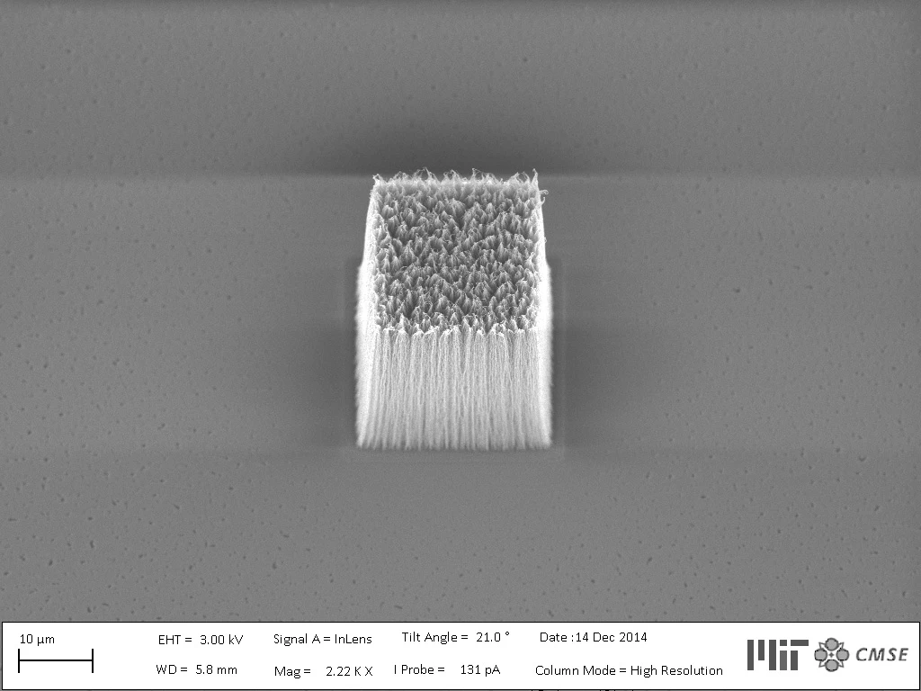
The researchers made the stamps by growing carbon nanotubes in a variety of patterns on a silicon surface. These tubes were then coated with a thin polymer layer to ensure two things: an even penetration of ink which contained nanoparticles such as silver, zinc oxide or semiconductor quantum dots, as well as to prevent shrinkage of the nanotubes after it was stamped.
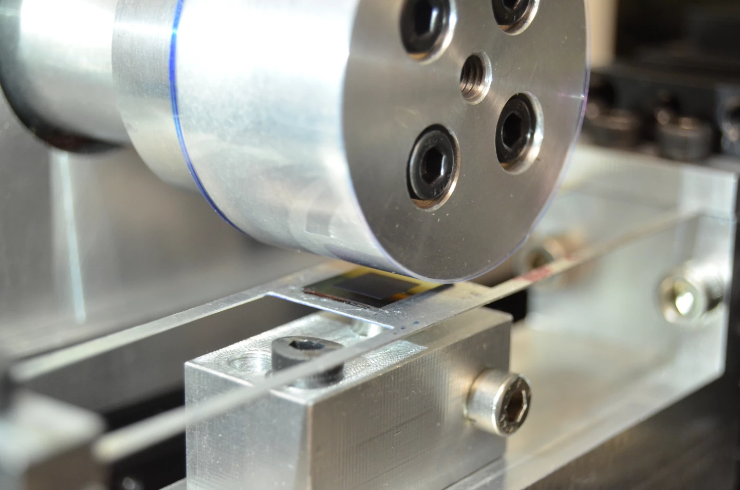
Since the amount of pressure applied when stamping the ink is also a key criterion for ensuring precise high-resolution patterns, the researchers developed a model to gauge the amount of force they would need to ensure an even layer of ink on each substrate. Using this information, they built a printing machine to mimic the industrial process and test the process. Despite the limitations of its roller, the results were actually comparable to the rates of existing industrial printing technologies.
"We found, limited by the motor we used in the printing system, we could print at 200 millimeters per second, continuously, which is already competitive with the rates of industrial printing technologies," says Hart. "This, combined with a tenfold improvement in the printing resolution that we demonstrated, is encouraging."
Importantly, the printed patterns were also found to be highly conductive and suitable for applications such as high-performance transparent electrodes.
"Our new printing process is an enabling technology for high-performance, fully printed electronics, including transistors, optically functional surfaces, and ubiquitous sensors," says Hart, adding that his team will be working to integrate the new technology with 2D materials such as graphene, "which together could enable new, ultrathin electronic and energy conversion devices."
You can read the results of their findings in Science Advances.
Source: MIT