The Internet of Things promises convenience, marked improvements in efficiencies, and huge economic benefits, but for such visions to be realized the number of physical devices being integrated with the digital world needs to continue increasing. But limiting the expansion, and ultimate ubiquity, of this technology has been the cost, power and size of the enabling electronics – all things that have been addressed by a new fabrication method.
Researchers at Purdue University and the University of Virginia are just the latest to take on the challenge of getting physical objects connected to the IoT cheaper and easier. To this end, they've developed a new ultra-thin circuit fabrication method that promises to bring the IoT to pretty much any object you can slap a label onto.
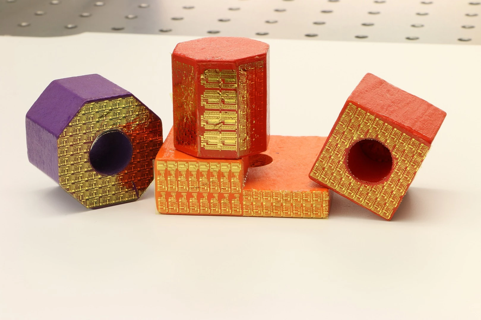
The process behind these peelable electronic circuits not only eliminates a number of manufacturing steps, thereby reducing cost, but it also means almost any object can act as a sensor or be controlled via the application of high-tech decals.

Of course, thin-film materials are nothing new, but this wafer-recyclable, transfer-printing process, using combinations of active nano-materials is a step into the future, both technologically and environmentally.
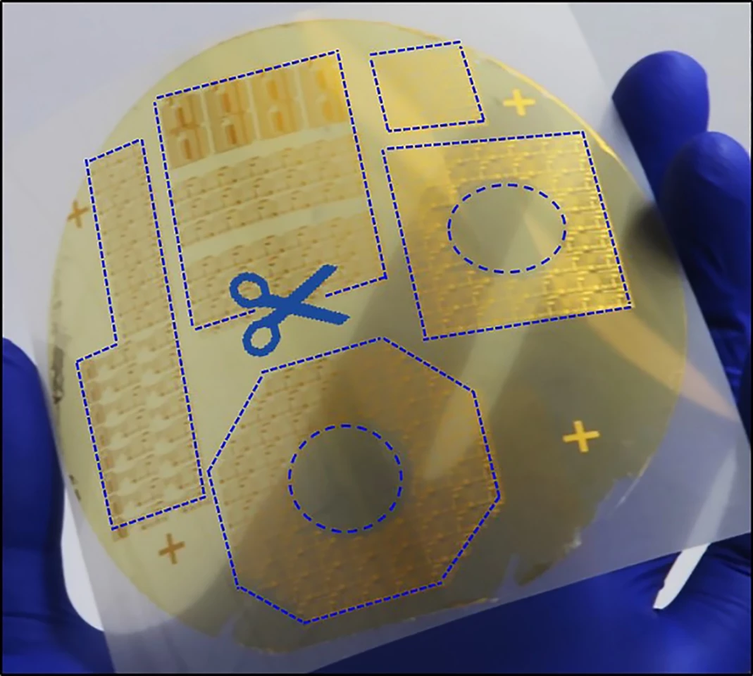
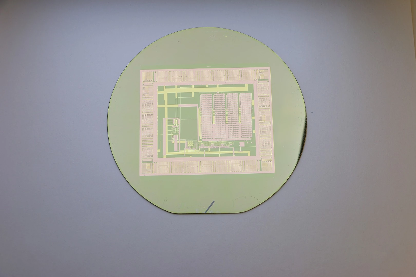
Conventionally, most electronic circuits are printed on rigid silicon wafers. These stiff substrates need to be resilient enough to withstand the heat and chemical etching of the process, and as such, the wafer is replaced each time a new circuit is printed. This new technique, called "transfer printing," allows a single wafer to be used over and over to build a near infinite number of flexible film-based circuits, which can be easily peeled off at room temperature by submerging the wafer and completed circuit in water.
"It's like the red paint on San Francisco's Golden Gate Bridge – paint peels because the environment is very wet," says Chi Hwan Lee, Purdue assistant professor of biomedical engineering and mechanical engineering. "So in our case, submerging the wafer and completed circuit in water significantly reduces the mechanical peeling stress and is environmentally friendly."

After the manufacturing process, the thin-film circuits can be trimmed to shape and stuck onto any suitable surface. "We've optimized this process so that we can delaminate electronic films from wafers in a defect-free manner," Lee says. Putting one of the stickers on a flower pot, for example, made that flower pot capable of sensing temperature changes that could affect the plant's growth.
According to the researchers, the stickers could eventually facilitate wireless communication. "We could customize a sensor, stick it onto a drone, and send the drone to dangerous areas to detect gas leaks, for example," says Lee.
The research was published in the journal PNAS and the process is demonstrated in the video below.
Source: Purdue University


