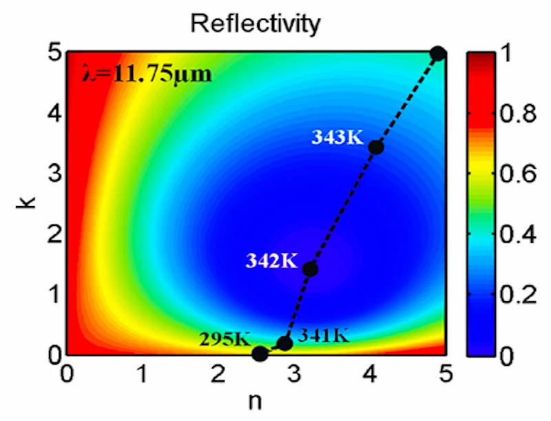
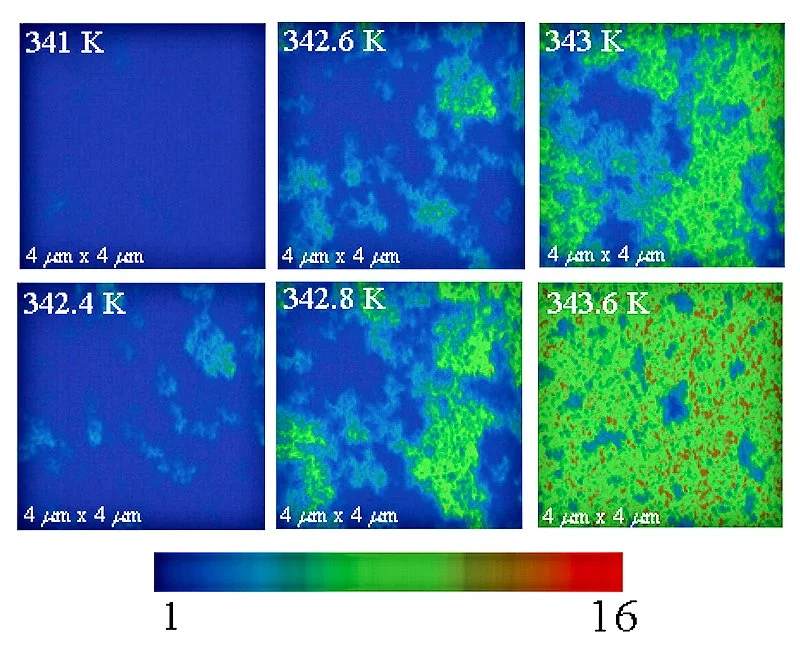
Harvard Professor of Applied Physics Federico Capasso and his collaborators have invented a nearly perfect optical absorber. By coating a piece of sapphire with an exceedingly thin 180-nm layer of vanadium dioxide, a surface is created that absorbs 99.75 percent of infrared light with a wavelength of 11.6 micron wavelength. Such optical absorbers can be tailored to enable a wide range of applications.
For most of a century, anti-reflection coatings have been used to greatly reduce reflections from an optical surface by creating destructive interference between the light waves reflected from the front and back interfaces of the coating. Essentially no light is lost to absorption in these conventional coatings.
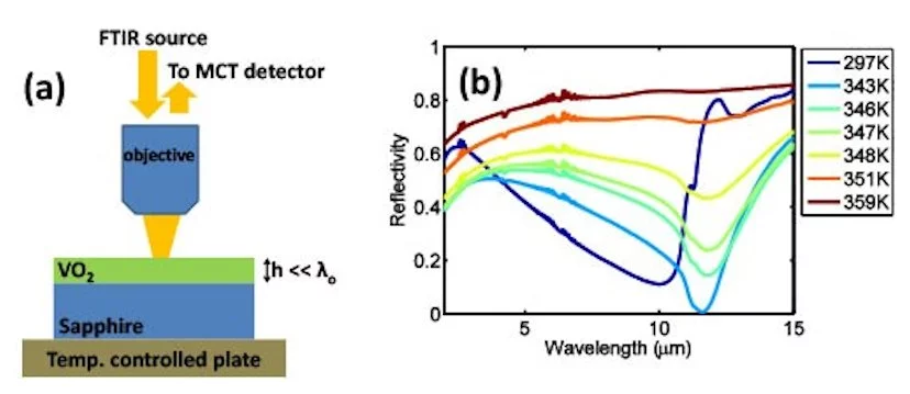
In contrast, Capasso's new class of absorbers still uses interference, but in this case the interference effects concentrate the light hitting the surface onto an ultra-thin layer of lossy material, which eventually absorbs all the light. The overall result is that the layer of vanadium dioxide (VO2), which by itself would reflect about three-quarters of the light, now absorbs all but 0.25 percent of that light.
VO2 undergoes a metal-insulator phase transition at temperatures reasonably near room temperature. The transition occurs at about 341 K, but can be tuned by changing composition, inducing mechanical stress, or subjecting the material to an electric field, changes in illumination, or other forms of electronic stimulus. This transition makes VO2 a prime candidate for a wide range of electrooptical devices, including memristors, smart mirrors, and optical switches.
When the VO2's temperature is close to the transition temperature, its electronic properties are dominated by electron correlation effects. Repulsion between electrons means that the freedom of a given electron to move depends to some extent on where the other electrons are and how they are moving.
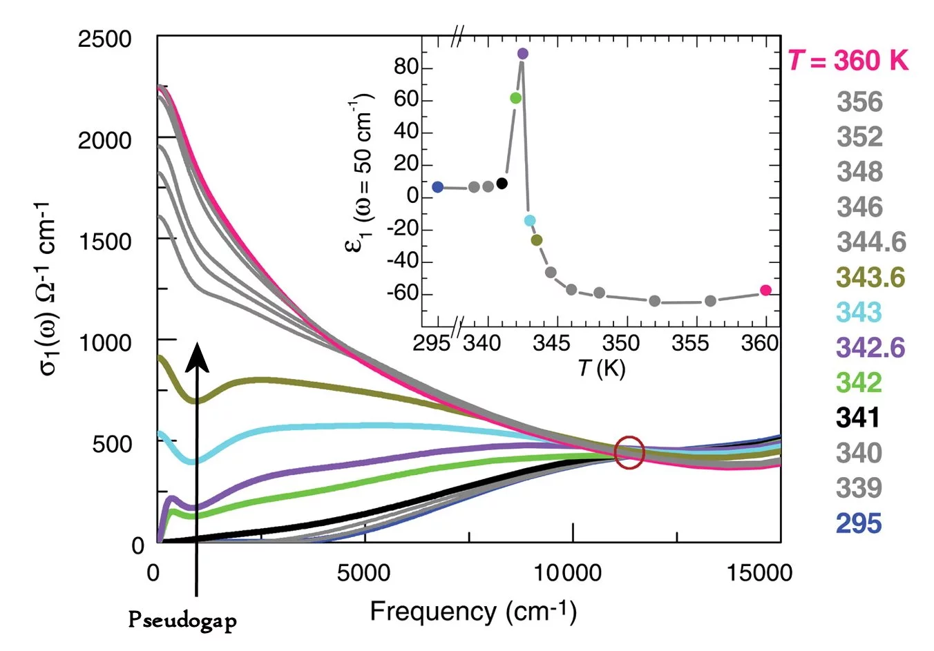
Electron correlation causes a substantial reduction in the number of electron states near a characteristic energy. Rapidly changing optical responses near this energy provides the VO2 with the properties needed for the perfect absorber. This is why the energy of the most highly absorbed light is about the same as the characteristic energy for electron state reduction.
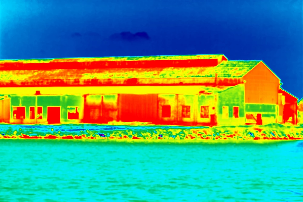
While a perfect absorber that works at one light frequency while held at a specific operating temperature may be a fascinating phenomenon, practical applications may not seem likely. Let's put up an example to consider. Detection of infrared and terahertz radiation is often carried out using bolometers - devices which detect radiation by measuring a temperature rise when incident radiation is absorbed. Arrays of bolometers are commonly used as image sensors. In fact, many thermal imaging cameras use VO2 bolometers.
A bolometer consists of a material heated by absorbing radiation and some means to measure changes in temperature. Immediately, a perfect absorber clearly results in greater detection sensitivity. In the Capasso group's absorber only a very thin film accomplishes the absorption, giving the bolometer very small thermal mass. This leads to larger changes in temperature, and again to greater sensitivity, as well as rapid response rates, making the recording of videos possible.
If the perfect absorption effect can be tuned over a range of frequencies, "color" photos and videos become possible, where the colors are light from different infrared or terahertz frequency bands. This would allow the enormous diagnostic power of multispectral imaging to be applied to new medical and security scans.
Improved bolometers are only one example of a potentially practical application. In any event, Capasso's remarkably clear demonstration of the basic physics of perfect absorption is likely to inspire a wide range of practical infrared and terahertz applications.
Sources: Applied Physics Letters and the University of California at San Diego


