
Moore's Law, which says that the number of transistors on a computer chip will double every two years or so, has managed to hold true for decades. But we're starting to bump up against the physical limits for how small these components can get. Now, engineers from MIT and the University of Colorado have developed a new microfabrication technique and used it to produce the smallest 3D transistors ever made, measuring about a third the size of the current leading commercial products.
Just a few years ago the industry standard for chips was 14 nanometers (nm), which describes the width of each transistor. Commercially, it's now 10 nm and quickly moving over to 7 nm, most notably in Apple's A12 Bionic processor, which powers the iPhone XR, XS and XS Max. IBM, meanwhile, has already begun to experiment with 5-nm chips.
Some of the new transistors developed by the researchers halve that again, measuring a record-setting 2.5 nm wide. To make them, the team modified a fairly-recently developed microfabrication method known as thermal atomic layer etching (thermal ALE). They start with an alloyed semiconductor material called indium gallium arsenide, then expose it to hydrogen fluoride, which creates a thin layer of metal fluoride on the substrate surface.
Next, the team adds an organic compound called dimethylaluminum chloride (DMAC), which triggers a chemical reaction known as ligand exchange. Ions called ligands in the DMAC bind to atoms in the metal fluoride layer, so when the DMAC is cleared away it strips individual atoms off the metal surface. As little as 0.2 nm is carved away each time, allowing incredibly precise etching when the process is repeated hundreds of times.
"You're kind of peeling an onion, layer by layer," says Wenjie Lu, first author of the study. "In each cycle, we can etch away just two percent of a nanometer of a material. That gives us super high accuracy and careful control of the process."
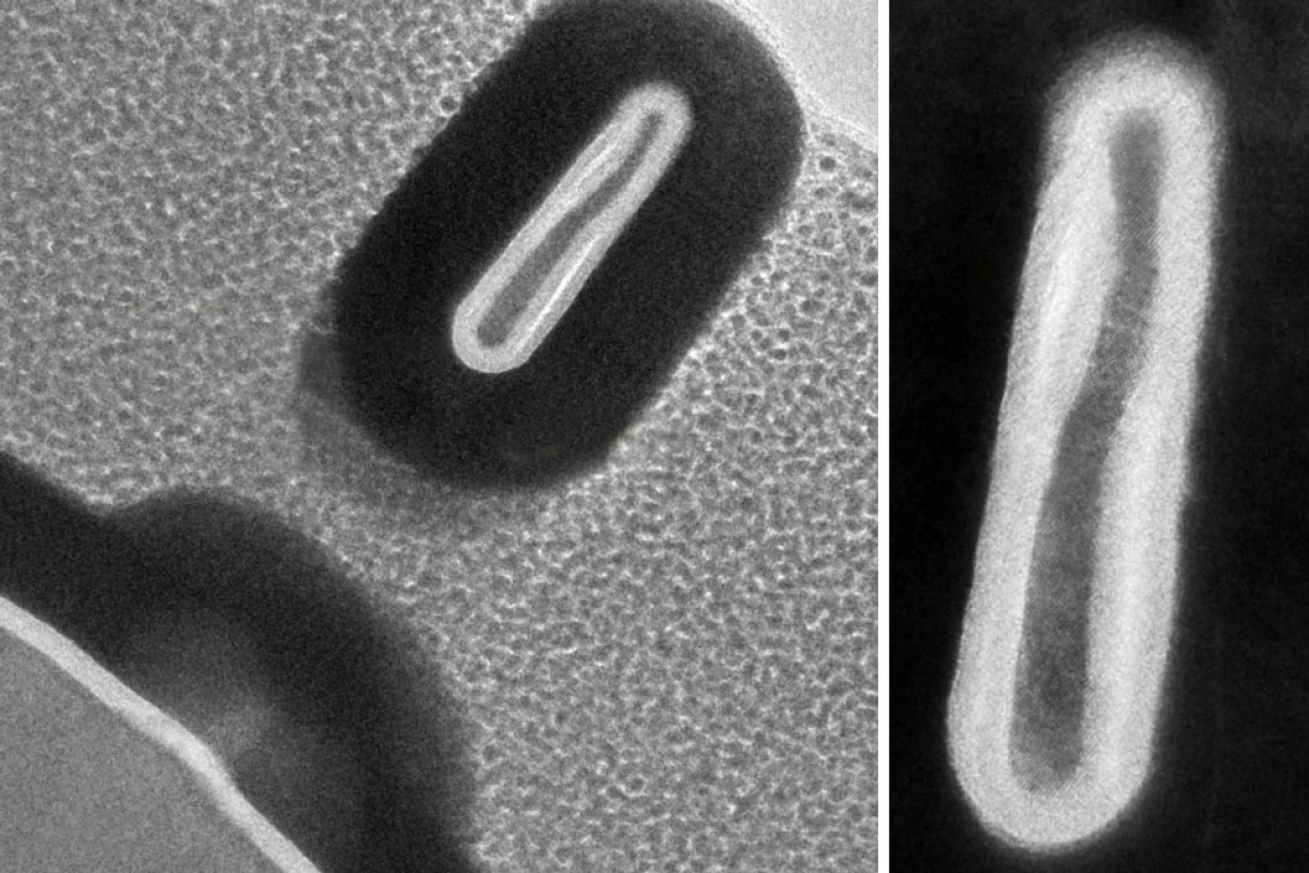
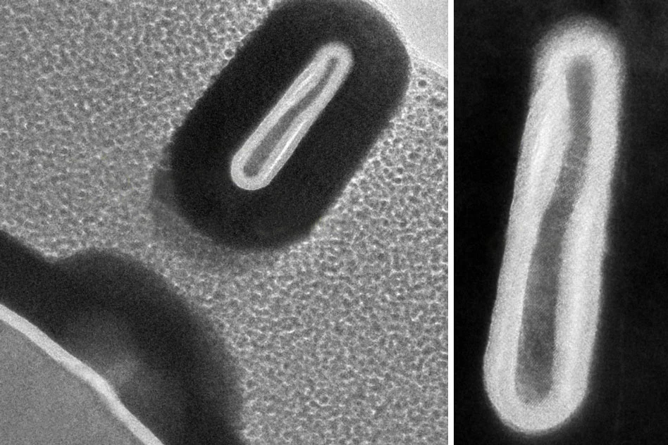
The researchers used the technique to fabricate FinFETs (Fin Field-effect transistors), the 3D transistors commonly used in commercial electronics. Most of these transistors measured less than 5 nm wide, with the smallest getting down to just 2.5 nm. On top of that, the team found that they performed up to 60 percent better than existing FinFETs and had a higher on-off contrast, making them more energy efficient. Both of these stats are thanks to the fabrication method, which reduces the number of defects introduced.
"We believe that this work will have great real-world impact," says Lu. "As Moore's Law continues to scale down transistor sizes, it is harder to manufacture such nanoscale devices. To engineer smaller transistors, we need to be able to manipulate the materials with atomic-level precision."
The research was presented at the IEEE International Electron Devices Meeting last week.
Source: MIT

